Journals > > Topics > Optics at Surfaces
Optics at Surfaces|35 Article(s)
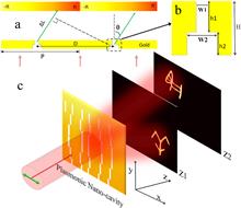
Control amplitude and phase of light by plasmonic meta-hologram with T-shaped nano-cavity
Wei Song, Shanguang Zheng, Yanan Fu, Changjun Min... and Xiaocong Yuan|Show fewer author(s)
Controlling both amplitude and phase of light in the subwavelength scale is a challenge for traditional optical devices. Here, we propose and numerically investigate a novel plasmonic meta-hologram, demonstrating broadband manipulation of both phase and amplitude in the subwavelength scale. In the meta-hologram, phase modulation is achieved by the detour phase distribution of unit cells, and amplitude is continuously modulated by a T-shaped nano-cavity with tunable plasmonic resonance. Compared to phase-only holograms, such a meta-hologram could reconstruct three-dimensional (3D) images with higher signal-to-noise ratio and better image quality, thus offering great potential in applications such as 3D displays, optical communications, and beam shaping. Controlling both amplitude and phase of light in the subwavelength scale is a challenge for traditional optical devices. Here, we propose and numerically investigate a novel plasmonic meta-hologram, demonstrating broadband manipulation of both phase and amplitude in the subwavelength scale. In the meta-hologram, phase modulation is achieved by the detour phase distribution of unit cells, and amplitude is continuously modulated by a T-shaped nano-cavity with tunable plasmonic resonance. Compared to phase-only holograms, such a meta-hologram could reconstruct three-dimensional (3D) images with higher signal-to-noise ratio and better image quality, thus offering great potential in applications such as 3D displays, optical communications, and beam shaping.
Chinese Optics Letters
- Publication Date: Jun. 10, 2019
- Vol. 17, Issue 6, 062402 (2019)


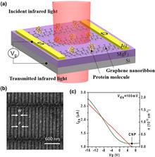
Detecting molecular vibrational modes of side chains and endpoints in nanoscale proteins with graphene plasmon
Chenchen Wu, Ning Liu, Hai Hu, Xiangdong Guo... and Qing Dai|Show fewer author(s)
Monitoring the chemical and structural changes in protein side chains and endpoints by infrared (IR) spectroscopy is important for studying the chemical reaction and physical adsorption process of proteins. However, the detection of side chains and endpoints in nanoscale proteins is still challenging due to its weak IR response. Here, by designing a double layered graphene plasmon sensor on MgF2/Si substrate in the IR fingerprint region, we detect the vibrational modes in side chains and endpoints (1397 cm 1 and 1458 cm 1) of monolayer protein. The sensor could be applied on biochemistry to investigate the physical and chemical reaction of biomolecules. Monitoring the chemical and structural changes in protein side chains and endpoints by infrared (IR) spectroscopy is important for studying the chemical reaction and physical adsorption process of proteins. However, the detection of side chains and endpoints in nanoscale proteins is still challenging due to its weak IR response. Here, by designing a double layered graphene plasmon sensor on MgF2/Si substrate in the IR fingerprint region, we detect the vibrational modes in side chains and endpoints (1397 cm 1 and 1458 cm 1) of monolayer protein. The sensor could be applied on biochemistry to investigate the physical and chemical reaction of biomolecules.
Chinese Optics Letters
- Publication Date: Jun. 10, 2019
- Vol. 17, Issue 6, 062401 (2019)
Parametric resonances in nonlinear plasmonics [Invited]|On the Cover
Shima Fardad, Eric Schweisberger, and Alessandro Salandrino
In the context of nonlinear plasmonics, we review the recently introduced concept of plasmonic parametric resonance (PPR) and discuss potential applications of such phenomena. PPR arises from the temporal modulation of one or more of the parameters governing the dynamics of a plasmonic system and can lead to the amplification of high-order sub-radiant plasmonic modes. The theory of PPR is reviewed, possible schemes of implementation are proposed, and applications in optical limiting are discussed. In the context of nonlinear plasmonics, we review the recently introduced concept of plasmonic parametric resonance (PPR) and discuss potential applications of such phenomena. PPR arises from the temporal modulation of one or more of the parameters governing the dynamics of a plasmonic system and can lead to the amplification of high-order sub-radiant plasmonic modes. The theory of PPR is reviewed, possible schemes of implementation are proposed, and applications in optical limiting are discussed.
Chinese Optics Letters
- Publication Date: Dec. 05, 2019
- Vol. 17, Issue 12, 122402 (2019)
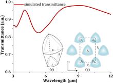
Broadband mid-IR antireflective Reuleaux-triangle-shaped hole array on germanium
Haijuan Cheng, Miao Dong, Qinwen Tan, Linghai Meng... and Lingxue Wang|Show fewer author(s)
A gradient-index Reuleaux-triangle-shaped hole array was fabricated on germanium (Ge) by nanoimprint lithography and inductively coupled plasma processing as a broadband mid-infrared (IR) antireflective surface. The interaction between the {111} planes of cubic crystalline Ge and a circular mold successfully produced an orderly and periodically distributed Reuleaux-triangle-shaped hole array. As a result, the average transmittance increased 15.67% over the waveband at 3–12 μm and remained stable at the incidence angle of up to 60°. The vertices of the Reuleaux triangle showed local enhancement of the electric field intensities due to interference of the incident and reflected radiation fields. It was also found that nonuniform hole depths acted to modulate the transmittance over the 3–12 μm waveband. A gradient-index Reuleaux-triangle-shaped hole array was fabricated on germanium (Ge) by nanoimprint lithography and inductively coupled plasma processing as a broadband mid-infrared (IR) antireflective surface. The interaction between the {111} planes of cubic crystalline Ge and a circular mold successfully produced an orderly and periodically distributed Reuleaux-triangle-shaped hole array. As a result, the average transmittance increased 15.67% over the waveband at 3–12 μm and remained stable at the incidence angle of up to 60°. The vertices of the Reuleaux triangle showed local enhancement of the electric field intensities due to interference of the incident and reflected radiation fields. It was also found that nonuniform hole depths acted to modulate the transmittance over the 3–12 μm waveband.
Chinese Optics Letters
- Publication Date: Dec. 10, 2019
- Vol. 17, Issue 12, 122401 (2019)
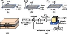
Optical rectification in surface layers of germanium
Li Zhang, Fangye Li, Shuai Wang, Qi Wang... and Gang Jia|Show fewer author(s)
In this Letter, we have demonstrated significant electric field induced (EFI) optical rectification (OR) effects existing in the surface layers of germanium (Ge) and measured the distributions of EFI OR signals along the normal directions of surface layers of Ge samples. Based on the experimental results, the ratios of the two effective second-order susceptibility components χzzz(2eff)/χzxx(2eff) for Ge(001), Ge(110), and Ge(111) surface layers can be estimated to be about 0.92, 0.91, and 1.07, respectively. The results indicate that the EFI OR can be used for analyzing the properties on surface layers of Ge, which has potential applications in Ge photonics and optoelectronics. In this Letter, we have demonstrated significant electric field induced (EFI) optical rectification (OR) effects existing in the surface layers of germanium (Ge) and measured the distributions of EFI OR signals along the normal directions of surface layers of Ge samples. Based on the experimental results, the ratios of the two effective second-order susceptibility components χzzz(2eff)/χzxx(2eff) for Ge(001), Ge(110), and Ge(111) surface layers can be estimated to be about 0.92, 0.91, and 1.07, respectively. The results indicate that the EFI OR can be used for analyzing the properties on surface layers of Ge, which has potential applications in Ge photonics and optoelectronics.
Chinese Optics Letters
- Publication Date: Oct. 10, 2018
- Vol. 16, Issue 10, 102401 (2018)

Multiple directional enhanced light source through a periodic metal grating structure
Le Yu, Xiao Xiong, Di Liu, Lantian Feng... and Xifeng Ren|Show fewer author(s)
Higher emission rates and controllable emission direction are big concerns when it comes to finding a good single photon source. Recently, surface plasmons are introduced to this application, as they can manipulate and enhance the luminescence of single emitters. Here, we experimentally achieve a wide-area multiple directional enhanced light source through periodic metal grating structures. The surface-plasmon-coupled emission can have multiple precisely emission angles by just changing the period of the grating. Our result indicates that metal plasmonic grating can be used as a productive quantum device for unidirectional quantum light sources in quantum optics. Higher emission rates and controllable emission direction are big concerns when it comes to finding a good single photon source. Recently, surface plasmons are introduced to this application, as they can manipulate and enhance the luminescence of single emitters. Here, we experimentally achieve a wide-area multiple directional enhanced light source through periodic metal grating structures. The surface-plasmon-coupled emission can have multiple precisely emission angles by just changing the period of the grating. Our result indicates that metal plasmonic grating can be used as a productive quantum device for unidirectional quantum light sources in quantum optics.
Chinese Optics Letters
- Publication Date: Aug. 10, 2017
- Vol. 15, Issue 8, 082401 (2017)
Optical rectification and Pockels effect as a method to detect the properties of Si surfaces
Qi Wang, Li Zhang, Xin Wang, Haiyan Quan... and Shaowu Chen|Show fewer author(s)
The depth profile of electric-field-induced (EFI) optical rectification (OR) and EFI Pockels effect (PE) in a Si(110) crystal are investigated. The results show that EFI OR and PE signals are very sensitive to the electric field strength in the surface layers of the Si crystal. Theoretical formulas that include the electric field parameters and the widths of the space-charge region are presented and agreed very well with the experimental results. The experiments and simulations indicate that EFI OR and PE are potential methods for researching the surface/interface properties along the depth direction in centrosymmetric crystals such as Si. The depth profile of electric-field-induced (EFI) optical rectification (OR) and EFI Pockels effect (PE) in a Si(110) crystal are investigated. The results show that EFI OR and PE signals are very sensitive to the electric field strength in the surface layers of the Si crystal. Theoretical formulas that include the electric field parameters and the widths of the space-charge region are presented and agreed very well with the experimental results. The experiments and simulations indicate that EFI OR and PE are potential methods for researching the surface/interface properties along the depth direction in centrosymmetric crystals such as Si.
Chinese Optics Letters
- Publication Date: Jun. 10, 2017
- Vol. 15, Issue 6, 062401 (2017)
Observing the spin Hall effect of pseudothermal light through weak measurement
Bin Cao, Dong Wei, Pei Zhang, Hong Gao, and Fuli Li
The spin Hall effect of light (SHEL) can be observed by the dark strip resulting from weak measurement. We find that the SHEL of a partially coherent beam (PCB) has a similar phenomenon as well. However, the dark strip in the SHEL of a PCB cannot be explained by considering the beam as an assemblance of coherent speckles. Also, the dark strip in a PCB is not purely dark. By analyzing the autocorrelation, we show that the SHEL of a PCB is the result of overlapping coherent speckles’ SHEL. We further prove our conclusion by adjusting convergence and incident angles. Finally, we develop a qualitative theory to clarify the SHEL of a PCB. The spin Hall effect of light (SHEL) can be observed by the dark strip resulting from weak measurement. We find that the SHEL of a partially coherent beam (PCB) has a similar phenomenon as well. However, the dark strip in the SHEL of a PCB cannot be explained by considering the beam as an assemblance of coherent speckles. Also, the dark strip in a PCB is not purely dark. By analyzing the autocorrelation, we show that the SHEL of a PCB is the result of overlapping coherent speckles’ SHEL. We further prove our conclusion by adjusting convergence and incident angles. Finally, we develop a qualitative theory to clarify the SHEL of a PCB.
Chinese Optics Letters
- Publication Date: Feb. 10, 2017
- Vol. 15, Issue 2, 022401 (2017)
Propagation properties of the terahertz waveguide using a metallic nanoslit narrower than skin depth
Jie Yang, Gongwei Lin, Yueping Niu, Yihong Qi... and Shangqing Gong|Show fewer author(s)
A terahertz (THz) waveguide using a metallic nanoslit whose width is much smaller than the skin depth is analytically investigated. By taking some important physical properties into account, we derive a simple, yet accurate, expression for the effective index. We also study the changes in modal field and the attenuation coefficient in the whole THz region, and find some interesting physical properties. Finally, we verify that these theoretical analyses coincide with the rigorous numerical simulations. This research can be useful for various applications of THz waveguides made of metallic nanoslits. A terahertz (THz) waveguide using a metallic nanoslit whose width is much smaller than the skin depth is analytically investigated. By taking some important physical properties into account, we derive a simple, yet accurate, expression for the effective index. We also study the changes in modal field and the attenuation coefficient in the whole THz region, and find some interesting physical properties. Finally, we verify that these theoretical analyses coincide with the rigorous numerical simulations. This research can be useful for various applications of THz waveguides made of metallic nanoslits.
Chinese Optics Letters
- Publication Date: Jul. 10, 2016
- Vol. 14, Issue 7, 072401 (2016)
Influence of surface roughness on surface plasmon resonance phenomenon of gold film
Zhitao Yang, Changjian Liu, Yachen Gao, Jiyu Wang, and Wenlong Yang
We experimentally investigate the effects of the surface roughness of gold thin films on the properties of surface plasmon resonance. By annealing at different temperatures, film samples with different surface morphologies are obtained. Specifically, due to the diffusion of the gold atoms towards the films’ surface, the surface root-mean-square roughness decreases with the increasing annealing temperature. Then, we measure the surface plasmon resonance of the samples. The results show that the resonance angle of the surface plasmon resonance is sensitive to the root-mean-square roughness, and it gradually decreases by reducing the surface root-mean-square roughness. We experimentally investigate the effects of the surface roughness of gold thin films on the properties of surface plasmon resonance. By annealing at different temperatures, film samples with different surface morphologies are obtained. Specifically, due to the diffusion of the gold atoms towards the films’ surface, the surface root-mean-square roughness decreases with the increasing annealing temperature. Then, we measure the surface plasmon resonance of the samples. The results show that the resonance angle of the surface plasmon resonance is sensitive to the root-mean-square roughness, and it gradually decreases by reducing the surface root-mean-square roughness.
Chinese Optics Letters
- Publication Date: Apr. 10, 2016
- Vol. 14, Issue 4, 042401 (2016)
Topics
- <
- 1
- 2
- 3
- 4
- >

© Copyright 2018-2021 | Chinese Laser Press. All Rights Reserved 沪ICP备15018463号-20